
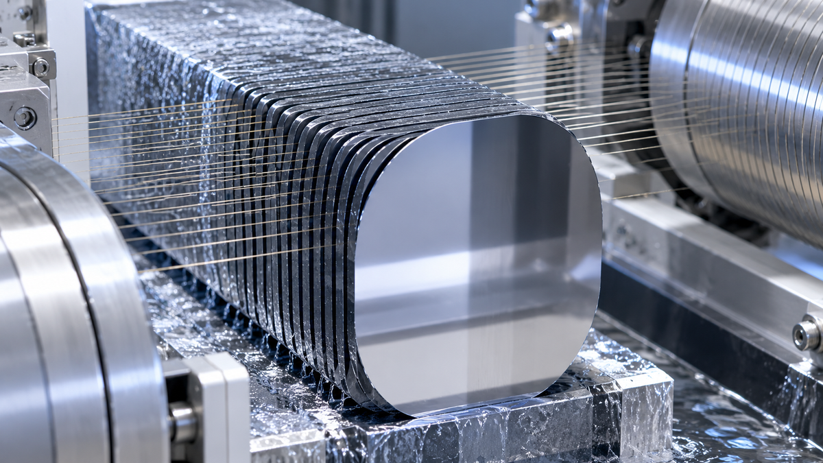
A specific thin-wafer case, clearly dated
Thinner silicon wafers are a manufacturing development to track, but a single company result should not be converted into an industry-wide 2026 specification. Risen Energy’s white paper, dated December 2023, says its HJT Hyper-ion cells used 110 μm silicon wafers and reports production milestones from April 27 to June 27, 2023. This article treats that as a named, dated case—not evidence that all HJT lines or all cell architectures use that thickness.
The distinction is important because wafer thickness can vary by product generation, cell route, wafer size, line capability and time. A figure that accurately describes one production program may be misleading when repeated without its manufacturer, product context and date.
What Risen’s white paper reports
The paper describes Risen’s HJT Hyper-ion development and industrial application of ultra-thin silicon wafers. It identifies 110 μm wafers for the company’s cells and says initial production began on April 27, 2023, with full-scale production reached on June 27, 2023. Those are company-reported details for that specific program. The paper does not establish a universal wafer-thickness range for the 2026 PV market.
The same document explains that reducing wafer thickness changes how wafers behave during production and handling, and that equipment, fixtures and automation may need adjustment. That observation is a useful manufacturing lesson: a material reduction is not isolated from yield, handling and line design. It does not, by itself, quantify a universal cost or carbon saving per watt.
Why slicing and handling must be considered together
Diamond-wire sawing is part of the wafering process, while wafer thickness describes the resulting silicon substrate. These are related but distinct variables. A thinner wafer can mean less silicon in an individual wafer, yet the manufacturing outcome also depends on kerf, breakage, cell conversion efficiency, yield, wafer dimensions and the energy and materials used across production. A reduction in thickness alone does not prove lower cost or lower lifecycle emissions per delivered watt.
The 2026 ITRPV is a current roadmap reference for trends across the crystalline-silicon photovoltaic value chain. Its existence provides a place to follow evolving manufacturing practice; this article does not attribute the 110 μm Risen result to that roadmap or claim that the public summary specifies a universal 2026 thickness.
The process trade-off behind a thinner wafer
Reducing thickness increases the importance of controlled transport, support and alignment because thin silicon is more vulnerable to handling stress. The Risen paper discusses adaptations to wafer carriers and automation in its own production ramp. That makes the case relevant to equipment and quality teams, but the operational choices described there should not be assumed to match another factory’s tooling or yield target.
For buyers, the module datasheet rarely answers every cell-manufacturing question. If wafer thickness matters to a project’s sustainability claim, supply-chain requirement or qualification process, request a dated declaration tied to the offered model and ask how the supplier verifies production consistency. Avoid comparing a pilot result with a sustained commercial specification unless their measurement and production contexts are aligned.
Questions for suppliers and technical reviewers
Ask which wafer thickness applies to the offered cell and module, whether the stated value is nominal or a range, how it is measured, which product family it covers, and when the specification was valid. If the supplier gives a single number, confirm whether it describes a production sample, a best-performing lot or the routine product specification. Keep the model and datasheet revision with the answer.
For a process claim, ask what evidence supports it: thickness metrology, breakage and yield records, traceability, or third-party product qualification as applicable. These records answer different questions. A thickness declaration does not certify module reliability, and a module certification does not necessarily disclose wafer dimensions.
Keep the number attached to its source
The defensible takeaway is narrow but useful: Risen Energy documented a 110 μm HJT Hyper-ion case in a December 2023 white paper, alongside production milestones in 2023. It is a historical manufacturer-specific example, not a blanket description of today’s industry. Any newer thickness claim should be supported by its own dated product or process source.
Frequently asked questions
What wafer thickness does the cited Risen case report?
Risen Energy’s December 2023 white paper reports 110 μm silicon wafers for its HJT Hyper-ion cells. The value is specific to that company’s case.
Does 110 μm describe the whole HJT industry in 2026?
No. The source documents Risen’s 2023 program and does not establish a universal 2026 thickness for HJT or other cell architectures.
Does a thinner wafer automatically reduce cost per watt?
Not automatically. Cost per watt also depends on yield, breakage, efficiency, wafer size, process energy and other production inputs.
What should a buyer verify?
Tie any thickness claim to the exact cell or module model, source date, measurement basis and production status, and distinguish it from reliability or certification evidence.
Use the news as a project input, then verify the scope.
This News item is editorial context. Confirm the final datasheet, applicable standard, project conditions and acceptance evidence before changing a design or purchase decision.
Discuss a project implication